Table of Content
ToggleWhat is a Hard-Core Processor?
A hard-core processor is just like any other processor in terms of functionality and application. It has all the basic building blocks such as registers, memory interfaces, ALU etc. and is fully capable of performing general purpose computing tasks. However, unlike soft-core processors, it has a fixed design layout and is predesigned, pre-verified and optimized with a fixed set of resources. It is a ready-to-use solution that is mainly meant to be integrated as an IP block in an SoC or FPGA for specific applications that require a balance between design complexity, speed, power consumption and customization.

Why Do We Need Efficient Communication Between Hard-Core Processor and FPGA?
FPGA and processor interface has become vital to any digital design due to fast growing real-time applications like object detection, classification, audio and speech processing, sensor and actuator interfaces etc. and these applications need bulk of parallel processing and reconfigurable multimode systems. Furthermore, performance requirements such as customization, real-time responsiveness, scalability and resource sharing make it worthwhile to utilize the benefits offered by a processor and an FPGA.
Processor interface provides interface to real time applications while FPGA being a resource giant provides memory interface, protocol and data acquisition for flexible and parallel or serial interface.
Interface between a Hard-Core Processor and FPGA
FPGA can be attached to a processor as a synchronous or asynchronous memory module. Here we will briefly explain the attributes of asynchronous interface between FPGA and processor.
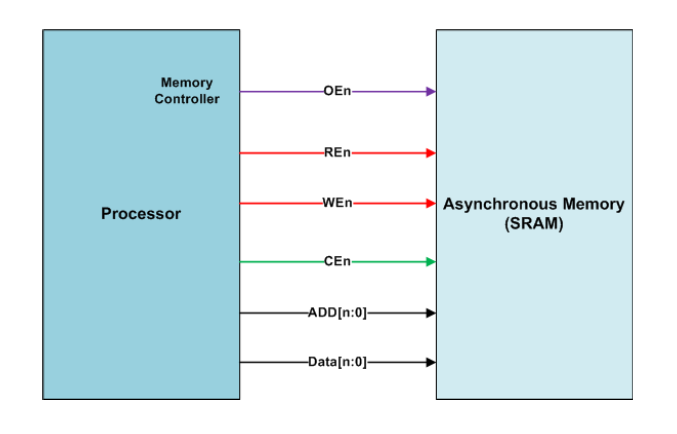
Processor has memory controllers that provide an interface to Asynchronous memories. This Asynchronous memory interface controls the transactions through control signals like CEn, WEn, REn, OEn, BEn, Address Bus and Bidirectional Data Bus.

Interface Between Processor and FPGA
On the processor side write process is controlled with the combination of WEn and CEn signals. Similarly, the read process is controlled with the combination of REn, CEn and OEn. Width of these signals is controlled on the processor side and dependent upon the processor’s system clock.
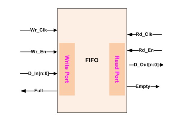
Whereas, in FPGA architecture there are built in Synchronous dual port FIFOs to store data. Write port of this port requires Wr_En, Wr_Clk, D_In[n:0] as input signals and Full as output/indicator signal. Read port requires Rd_En and Rd_Clk as input signal and D_Out[n:0] as output and Empty signal as control/indicator signal of Read process.

Synchronous Dual Port FIFO in FPGA
On the FPGA side data is written Synchronously i.e. on every edge of Wr_Clk assertion of Wr_En (Wr_En is combinational logic of WEn and CEn) is checked. It implies that the width of Wr_En controls the number of words being written. Full signal is asserted as an indication that FIFO is Full. And data is read Synchronously i.e. on every edge of Rd_Clk assertion of Rd_En (Rd_En is combinational logic of REn and CEn) is checked. It implies that the width of Rd_En controls the number of words being read. Empty signal is asserted as an indication that FIFO is empty.
The problem is that processor’s memory interface is Asynchronous and FPGA’s FIFO interface is Synchronous.
The performance of this FPGA-processor interface is limited by the width of Wr_En and Rd_En signals since Wr_En and Rd_En are generated by processor and dependent upon the operating frequency of processor’s Asynchronous interface.
There are two possible scenarios for this Asynchronous interface.
The operating frequency of processor’s Asynchronous interface is higher than the Wr_Clk and Rd_Clk on the FPGA side. Then forget about any data transaction under this condition.
Data transaction is possible iff the operating frequency of processor’s Asynchronous interface is of equal or lower than the operating frequency of dual port FIFO interface on FPGA side, sounds logical.
- The strobe width of WEn and REn on processor side should be kept at least one clock cycle of FPGA’s Wr_Clk and Rd_Clk respectively, which is the best ideal case.
- Most of the time it is not possible to keep the signals of one clock cycle on the processor side. In such situation on the FPGA side the generation of Wr_En and Rd_En is done accurately on one cycle of Wr_Clk and Rd_Clk respectively using combinational logic and respective clock edges.
Performance Benefits of Parallel Asynchronous Interface between a Hard-Core Processor and FPGA
A parallel asynchronous interface between a processor and FPGA have a number of key benefits to offer. Some of them include increased data throughput, improved parallel processing, lower latency, efficient resource utilization and scalability. These benefits make the combination of these two processing elements as an ideal choice in application where real-time performance, high performance computing, offloading computations and many other data intensive applications.


