Table of Content
ToggleHistory of Flash Memory
Masuoka Fujio, a Japanese engineer at the time working for Toshiba Corporation, devised flash memory in the early 1980s as a way to replace current data storage mediums such as magnetic tapes and floppy discs.
Ariizumi Shoji, a Masuoka co-worker, developed the term flash after comparing the method of memory erasure, which can delete all the data on a complete chip at once, to a camera’s flash [1].
What is a Flash Memory?
A non-volatile electronic memory storage media is known as flash memory. The term “non-volatile memory” refers to memory that retains data even after the system is turned off.
It’s employed in a wide range of devices and allows users to easily wipe and reprogram data. Examples of flash memory include digital audio players, personal computers, mobile phones, digital cameras, synthesizers, industrial robotics, video games, scientific instrumentation, and medical electronics.
Types of Flash
There are two types of flash available one is called NOR flash and the other is the NAND flash. NAND flash is further categorized into raw NAND and managed NAND.
These NOR and NAND flashes got their names from the logic gate they made up of, that’s why each has a different architecture and specialties.
NAND Flash vs NOR Flash
When choosing a Flash memory, embedded system designers must evaluate several factors, including the type of Flash, architecture to utilize, whether to use a serial or parallel interface and whether or not error correction code, wear leveling, etc is required. If just one type of interface is supported by the processor or controller, the alternatives are limited, making memory selection easier.
Architecture
NOR flash is designed for random access, which means it can access data in any order and does not need the user to follow a list of storage locations.
Each NOR Flash memory cell is connected in parallel in its internal circuit; one end of the memory cell is connected to the source line, while the other end is connected to the bit line as shown in Figure 1.
The system can now access individual memory cells as a result of this. This provides the benefit of random access and quick read speeds, making this an ideal choice for code execution [2].
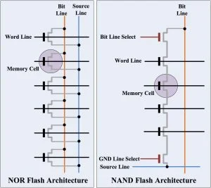
On the other hand, NAND flash is designed for high-density storage of data rather than random access. NAND Flash cells, unlike NOR Flash, are connected in a series to the bit line called a string, generally eight memory transistors at a time.
The drain of one cell is linked to the source of the following cell in this configuration as shown in Figure 1. Because of the series connection, the number of ground wires and bit lines is reduced, and it has a lower cell size as a result of this architecture. Direct access to individual cells is not possible, however [2].
Memory Density
Because NAND Flash has greater densities, it can store significantly more data. NAND Flash memory capacity range from 128MB to 2TB. This makes it ideal for data storage devices like Flash drives, digital cameras, and USB drives. NAND has smaller memory cells and can scale due to its higher densities [2].
In contrast to NAND, NOR Flash has a lower density and hence a lesser memory capacity. The density of NOR Flash memory generally ranges from 64MB to 2GB.
As a result, NOR flash is better suited to low-capacity, high-reliability applications, such as storing code in mobile phones and medical equipment. Furthermore, NOR has a bigger memory cell size than NAND, which restricts its scaling possibilities [2].
Write/Erase/Read Performance
The construction of NOR and NAND Flash has an impact on how well they write, erase, and read data. Short read times are possible because NOR Flash memory cells are wired in parallel and may be accessed immediately.
However, NOR Flash’s capacity to write and erase as rapidly as NAND Flash is hampered by its bigger cell size and more complex erasing procedure. [2].
In contrast, NAND memory cells, are connected in a series that is divided into pages, which are then sub-organized into blocks.
NAND readings are slower because it provides page and blocks access rather than random access hence, not able to read each byte separately. NAND writes and erases are, nonetheless, faster than NOR. [2].
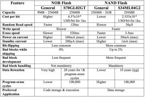
| Feature | NOR Flash | NAND Flash |
|---|---|---|
| Cost per bit | Higher | Lower |
| Random read speed | Faster | Slower |
| Write speed | Slower | Faster |
| Erase speed | Slower | Faster |
| Power on current | High | Low |
| Standby current | Low | High |
| Bit flip | Less common | More Common |
| Bad block while shipping | 0% | Up to 2% |
| Bad block development | Less frequent | More frequent |
| Bad block handling | Not mandatory | Mandatory |
| Data retention | Very high | Lower |
| Program-erase cycle | Lower | Higher |
| Preferred application | Code storage and execution | Data Storage |
NAND Flash
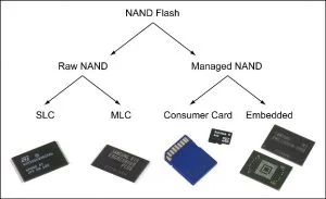
There are two primary types of NAND flashes: Raw NAND and Managed NAND. A NAND flash device can be broken up into three distinct parts.
Cell: The tiniest of things. The device managing the NAND storage cannot directly address a cell since it stores data at the bit level.
Page: For reading and writing operations, the smallest array of cells may be addressed. The “flipping” of bits from the value 1 to the value 0 is a program operation. Page sizes are measured in kilobytes, for example, 4 KB.
Block: The smallest array of pages to which erase operations can be addressed. In some cases, a block is also referred to as an erase block. Block sizes are measured in megabytes, for example, 4 MB. Over time, erase operations degrade flash storage. When a block can no longer be used to store data, it is labeled as a bad block.
The most essential takeaway from the preceding points is that blocks deteriorate as they are erased. The number that indicates how many times each block has been erased is known as the block erase count [5].
Raw NAND
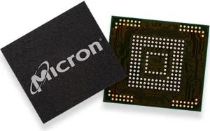
Raw NAND does have the lowest cost per bit, but all management operations must be performed by a separate host controller (not included in the package).
Bits are stored in a cell, which is the smallest unit. During a read operation, the voltage level thresholds it can retain and distinguish determine how many bits are saved per cell. The number of bits that the cells can store is indicated by various flash memory identifiers [5].
- SLC: single-level cell, stores 1 bit per cell
- MLC: multi-level cell, stores 2 bits per cell
- TLC: triple-level cell, stores 3 bits per cell
- QLC: quad-level cell, stores 4 bits per cell
There is a trade-off between density, cost, endurance, and performance, summarized in Figure 3.
Managed NAND
Managed NAND includes memory management into the package, simplifying the design-in process [7]. Managed NAND is a combo of raw NAND flash (SLC or MLC) and a hardware controller that performs flash management functions such as
- Wear levelling
- Bad block management
- ECC (Error Code correction)
Bad Block Management
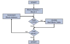
Due to production limits, NAND Flash devices are sold with faulty blocks scattered around. Before delivery, the locations of these initial faulty blocks are noted in the Flash device itself.
It is best to avoid using these bad blocks since they can cause damage to other good blocks. The information from these early defective blocks is stored in a bad block table on the host system [9].
Due to memory wear, NAND Flash devices will gather faulty blocks during their lifetime. When a program or wipe operation reports “Fail” in the status register, these extra faulty blocks can be found.
Failure to program one page in a block has no impact on the other pages in the block. Other pages in the block’s content are transferred to another good block, and the old block is labeled as bad.
The host system records this information in the bad block table to prevent the block from being used again [9].
Error Code Correction
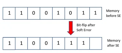
In Flash memory, bit-flipping refers to data corruption caused by occasional errors, in which the status of a bit seems to be flipped.
Any such flaws must be detected and corrected to protect the integrity of stored data. ECC (Error Correction Code) technology is a method of detecting and correcting faults in memory devices.
Error correction codes locate and rectify errors by adding redundant bits to data bits. For every m-bits of data, k-bits of redundant bits are added, resulting in m+k bits of effective data or coded data.
When an invalid codeword is found, the ECC method will encode these m+k bits, allowing any fault in the received data to be identified. A found error can be rectified based on the ECC algorithm’s capabilities.
Many error correction algorithms are widely used in different scenarios, each algorithm has some advantages and disadvantages over one another.
The most commonly used ECC algorithms in Flash memories are Hamming codes; Bose, Chaudhuri, and Hocquenghem (BCH) codes; Reed-Solomon (R-S) Codes; and Low-Density wwParity Codes (LDPC) [9].
Wear Leveling
Wear leveling methods are used by all managed NAND devices to work around program/erase constraints by organizing data and uniformly spreading writes throughout the whole block (so no single block fails due to intensive writes).
It avoids the overuse of blocks, allowing all blocks to be used to their full potential. As a result, wear leveling increases the memory device’s life and enhances its reliability and durability [12].
Managed NAND Examples
Because the controller is built into the package to handle wear leveling, bad block management, and ECC, managed NAND is much more durable and provides increased life expectancy. Check the datasheet of the product for exact life cycle information. Examples of managed NAND are as follows:
- eMMC
- SD card
- CompactFlash
- Solid State Drives
- Universal Flash Storage
Wear Estimation of NAND Flash
At any given time, flash health can be calculated as the amount of its capacity that has already been depleted. At first, just for simplicity, suppose that no blocks wear out prematurely, that wear leveling is optimum and constant, and that there is no write amplification – in other words, the ideal scenario.
- Estimate the amount of data that is written to the device per day/week/year.
- Know how many years you expect the device to operate.
TBW = (5 GB per day) x (365 days per year) x (10 years)
TBW = 18.25 TB written
Write amplification factor
The phenomenon of write amplification occurs when the amount of written physical data to the NAND flash exceeds the amount of data written by the host computer. Two main factors cause write amplification factor;
First, every memory storage device that utilizes NAND Flash memory is made of elements that must be erased before they can be rewritten again.
Second, while NAND storage devices can be written one at a time which is usually the size of a page is 4K bytes ~ 16 K bytes, they can only be erased one block at a time.
A block sometimes referred to as a “NAND block” or “erase block” may hold hundreds of pages. This necessitates background processes that transport stored user data inside.
As a solution, old data in NAND frees up neighboring pages of data that may be erased to make room for new data written by the host computer.
Therefore, the total number of real writes to a NAND flash is generally larger than the number of writes that the host computer intends to do. Mathematical representation is known as WAF [9].
Write Amplification Factor = (Data Written to the Flash Memory) / (Data Written by the host)
Typically, the WAF is in the range of 1.0 to 2.5. Write amplification can vary greatly depending on the nature of the data stream (or workload) from the host machine. Small-block random writes, on average, produce a greater WAF and more wear than large-block sequential writes.
Also, full Derives will experience a higher WAF compared to partially full drives. Optimizing workload to minimize WAF can Maximize the lifetime.

TBW with typical WAF
- Estimate the amount of data that is written to the device per day/week/year.
- Know how many years you expect the device to operate.
- Insert the write amplification factor.
- Perform the calculation.
TBW = (5 GB per day) x (365 days per year) x (10 years)
TBW = 18.25 TB written
TBW after WAF,
TBW = 18.25 TBW x 1.5 WAF
TBW = 27.325 TB written
If the device is 8GB, the required Program/ Erase cycles would be,
Program Erase Cycles = (27,325 GB) /(8 GB)
Program Erase Cycles = 3,422
If the device is only specified to 3,000 Program/ Erase Cycles your device will fail before 10 Years. Therefore, using a high-capacity device will resolve this.
References:
- E. Gregersen, “flash memory,” [Online]. [Accessed 15 12 2021].
- J. Hopkins, “Differences Between NAND vs NOR Flash Memory,” 9 June 2021. [Online]. [Accessed 15 12 2021].
- J. S. Meena, “Overview of Emerging Non-volatile Memory Technologies,” Sep 2014. [Online]. [Accessed 15 12 2021].
- A. Aravindan, “NAND Flash vs NOR Flash,” 23 July 2018. [Online]. [Accessed 15 12 2021].
- J.-L. AUFRANC, “Wear Estimation for Devices with eMMC Flash Memory,” 16 AUGUST 2019. [Online]. [Accessed 15 12 2021].
- E. Sullivan, “What are the NAND flash memory types and where do they work best?,” 27 Feb 2020. [Online]. [Accessed 15 12 2021].
- T. Denholm, “The Universe of Managed NAND,” [Online]. [Accessed 15 12 2021].
- zegobit, “embedded Multi Media Card” 1 May ’17 2017. [Online]. [Accessed 15 12 2021].
- A. Aravindan, “Error management in NAND Flash,” 31 March 2019. [Online]. [Accessed 15 12 2021].
- Transcend, “Bad Block Management,” [Online]. [Accessed 15 12 2021].
- D. Maric, “Are we going soft on errors?,” [Online]. [Accessed 15 12 2021].
- “How Wear Leveling Extends SSD Life Expectancy,” 5 8 2020. [Online]. [Accessed 15 12 2021].
- R. t. Micron, “Write Amplification,” 13 September 2016. [Online]. [Accessed 15 12 2021].
Facing challenges with flash memory selection for embedded applications or electronic product development in general? Feel free to Contact Us for hardware design, embedded development, and firmware consultancy.


