
This case study describes how Oxeltech designed the complete electronics module for a wearable AI necklace for the consumer wellness market. The challenge was fitting a dual-microphone audio system, Bluetooth 5.1 radio, 6-axis IMU, LRA haptic actuator, RGB LED, and SD card storage into a Ø30 mm × 6 mm internal enclosure with a metal housing that blocks RF signals.
1. Project overview
1.1 What the product does
It is a wearable necklace that connects to a companion mobile app over Bluetooth. The necklace captures the wearer’s voice using onboard microphones. AI inference is used to detect positive self-talk patterns, triggering a vibration as a physical affirmation signal. The device also measures breathing rate using an inertial measurement unit and stores audio locally on an SD card when the phone is not in range.
1.2 Oxeltech’s scope
The client owned the jewellery design, stone selection, and external aesthetics. Oxeltech was responsible for everything inside the enclosure: hardware architecture, component selection, PCB layout, and mechanical integration.
1.3 Business constraints
The electronics had to fit the existing enclosure geometry without changing the external form factor. That requirement defined every design decision that followed.
2. Constraints and challenges
2.1 Size
Total internal thickness: 6mm. Target component height: below 1mm wherever possible.
At this scale, height had to be evaluated before electrical performance for every part. Components that exceeded the height budget were rejected regardless of electrical fit. 2.2 RF and the faraday cage problem
The enclosure was initially fully metal. A metal shell acts as a Faraday cage and attenuates RF signals. To address this, the enclosure was redesigned as a metal composite and plastic polymer combination, creating a usable RF window for BLE transmission.
2.3 Power budget
Battery capacity: 185mAh.
The system runs continuous microphone sampling, periodic BLE transmission, IMU polling, and occasional haptic feedback from a single small cell. No peripheral could be allowed to dominate the power budget.
2.4 PCB density
All components had to coexist on one board inside 6mm. Standard 2-layer or 4-layer PCB design rules do not provide enough routing density. A 6-layer HDI stackup was required.
2.5 Mechanical integration
Standard connectors did not fit the enclosure geometry. The charging interface and board retention both required redesign around the physical constraints of the pendant form factor.
3. Technical decisions
3.1 MCU selection: nRF5340
The nRF5340 is a dual-core SoC:
- Application core: 128MHz Arm Cortex-M33
- Network core: 64MHz Arm Cortex-M33
- Integrated Bluetooth 5.2
- Configurable TX power: -20 to +3 dBm
Why dual-core matters here:
On the application core: audio sampling from the PDM microphones, IMU polling, SD card writes, power management, and LRA control.
On the network core: the BLE stack, exclusively.
On a single-core SoC, BLE interrupt handling competes with audio sampling and introduces jitter into the PDM stream, corrupting audio quality. The dual-core architecture eliminates this.
Configurable TX power gives the firmware the ability to reduce BLE transmission power when the phone is close. Lower TX power means lower current draw, which extends battery life without affecting connection quality.
Device firmware update (DFU) over BLE is supported, allowing field firmware updates without physical access to the device.
3.2 Antenna placement
The antenna is a PCB trace antenna placed with deliberate clearance from all surrounding copper pours, metal enclosure walls, and nearby components. This clearance reduces the shielding effect of the enclosure. No external antenna was used placement and the keep-out zone were the only tuning levers. BT 5.1 receiver sensitivity is -97.5 dBm; the link budget was validated against body-worn attenuation to confirm reliable connectivity.
3.3 Microphones: why two
Two microphones were used instead of one for noise cancellation. A wearable microphone always captures ambient noise, clothing contact, and movement alongside the voice. A dual-microphone arrangement allows the firmware to separate the voice signal from background noise, improving the reliability of self-talk detection on the app.
3.4 Audio routing: BLE vs SD card
When BLE is connected, Audio streams live to the mobile app.
When BLE is not connected, Audio writes automatically to the onboard microSDHC card.
When BLE reconnects: The device resumes live streaming.
The SD card is the offline buffer. No audio is lost during disconnection. The switchover is handled in firmware without user input.
SD-card specification:
- Capacity: 32GB
- Class: U3 / A2
- Speed: up to 30 MB/s
3.5 IMU power mode
The 6-axis IMU measures breathing rate by detecting chest movement.
Only the accelerometer is active during normal operation. The gyroscope is disabled.
Gyroscope data is not needed for breathing rate detection. Accelerometer-only mode below 50Hz ODR draws under 10µA, making IMU contribution to the total power budget negligible.
3.6 Vibration: LRA vs ERM
An LRA (Linear Resonant Actuator) was selected over an ERM motor.
LRA specifications:
- Drive frequency: 240Hz
- Drive voltage: 0.4VAC rms
- Minimum vibration: 0.12Grms
LRA offers faster response time, precise frequency control, and a smaller footprint than ERM. In a wellness wearable where haptic feedback must feel immediate and intentional, LRA is the correct choice.
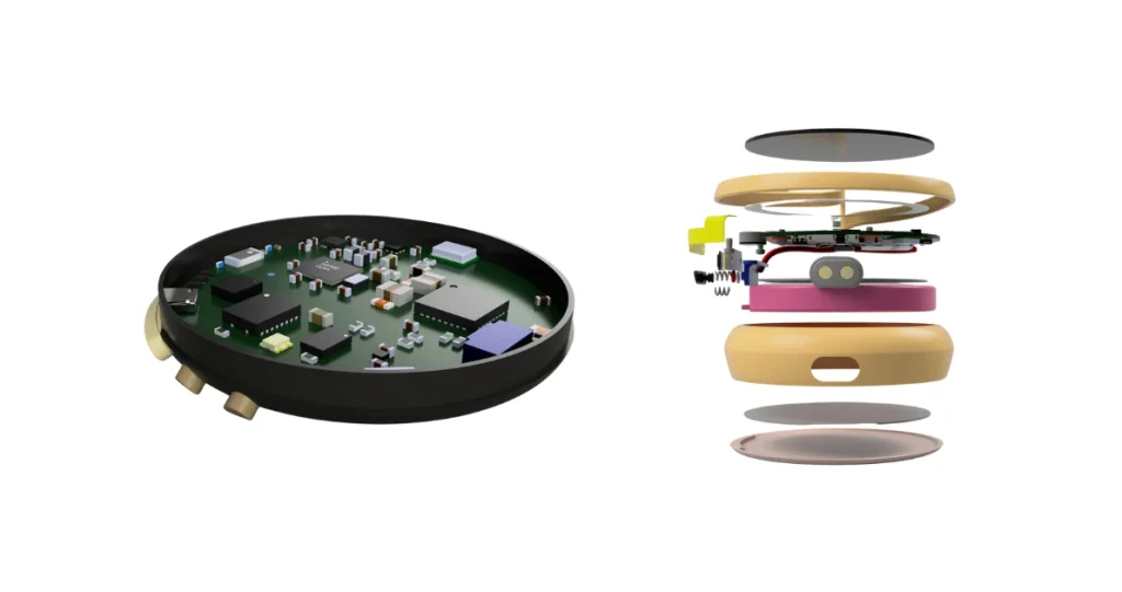
3.7 PCB: 6-layer HDI
Stackup: 6-layer HDI (High Density Interconnect)
Via types: Blind vias, buried vias, microvias
Why was HDI required?
Standard through-hole via PCBs cannot achieve the routing density required at 6mm internal thickness. HDI microvias are laser-drilled and far smaller, allowing full component density on both board sides without the space constraints of mechanical drill vias.
HDI microvias are laser-drilled and far smaller than mechanical drill vias. Blind vias connect outer layers to inner layers without passing through the full board. Buried vias connect inner layers to inner layers. Together, they allow full routing density in a board this thin.
Signal integrity was managed through star grounding, differential routing for PDM lines, controlled impedance for the BLE RF path, and proper ground plane stitching between layers.
Figure: AI necklace front view
4. Implementation
4.1 Component list
| Component | Part / Spec |
| MCU / SoC | nRF5340 (dual-core Cortex-M33, BT 5.1) |
| Microphones | 2x T5838 PDM, 16K, 65 dBA SNR |
| IMU | 6-axis, accelerometer-only mode <10µA |
| Vibration | LRA, 240Hz, 0.4VAC rms |
| Storage | microSDHC, 32GB, Class U3/A2 |
| LED | RGB, R:150mcd / G:600mcd / B:120mcd |
| Battery | 185mAh |
| PCB | 6-layer HDI, blind/buried microvias |
4.2 Power management
The nPM1300 from Nordic Semiconductor was selected as the PMIC. It is a natural pairing with the nRF5340 and handles battery charging and system power rail distribution in a compact 3.1×2.4mm WLCSP or 5x5mm QFN32 package.
Peripheral power states are managed in firmware:
- SD card: Active only when BLE is disconnected
- IMU: Accelerometer-only mode below 50Hz ODR during normal operation
- BLE TX power: Adjusted to the minimum required for the current connection quality
- LRA: Event-driven, negligible average current contribution
4.3 Mechanical redesign
Standard connectors did not satisfy the mechanical constraints of the pendant enclosure. The charging interface and board retention were redesigned specifically for this geometry. Multiple iterations were required before electrical and mechanical requirements were simultaneously satisfied.
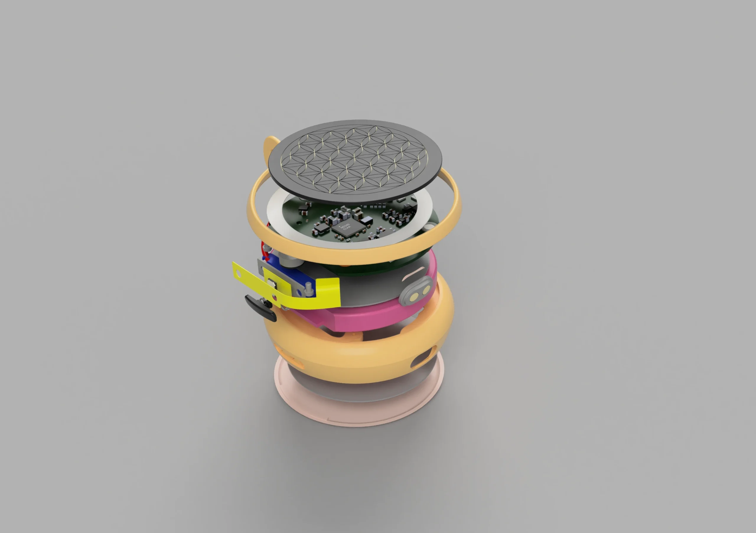
Figure: AI necklace assembly layers
5. Results
The electronics module fits within the 6mm internal thickness constraint without modifying the external jewellery form factor.
- BLE connectivity is functional through the metal enclosure using PCB antenna placement with clearance-based RF isolation
- Dual-microphone noise cancellation is active, improving voice detection reliability for the mobile app
- Audio automatically falls back to SD card when BLE disconnects, with no data loss
- IMU breathing rate measurement draws under 10µA in normal operation
- DFU over BLE enables firmware updates without physical device access
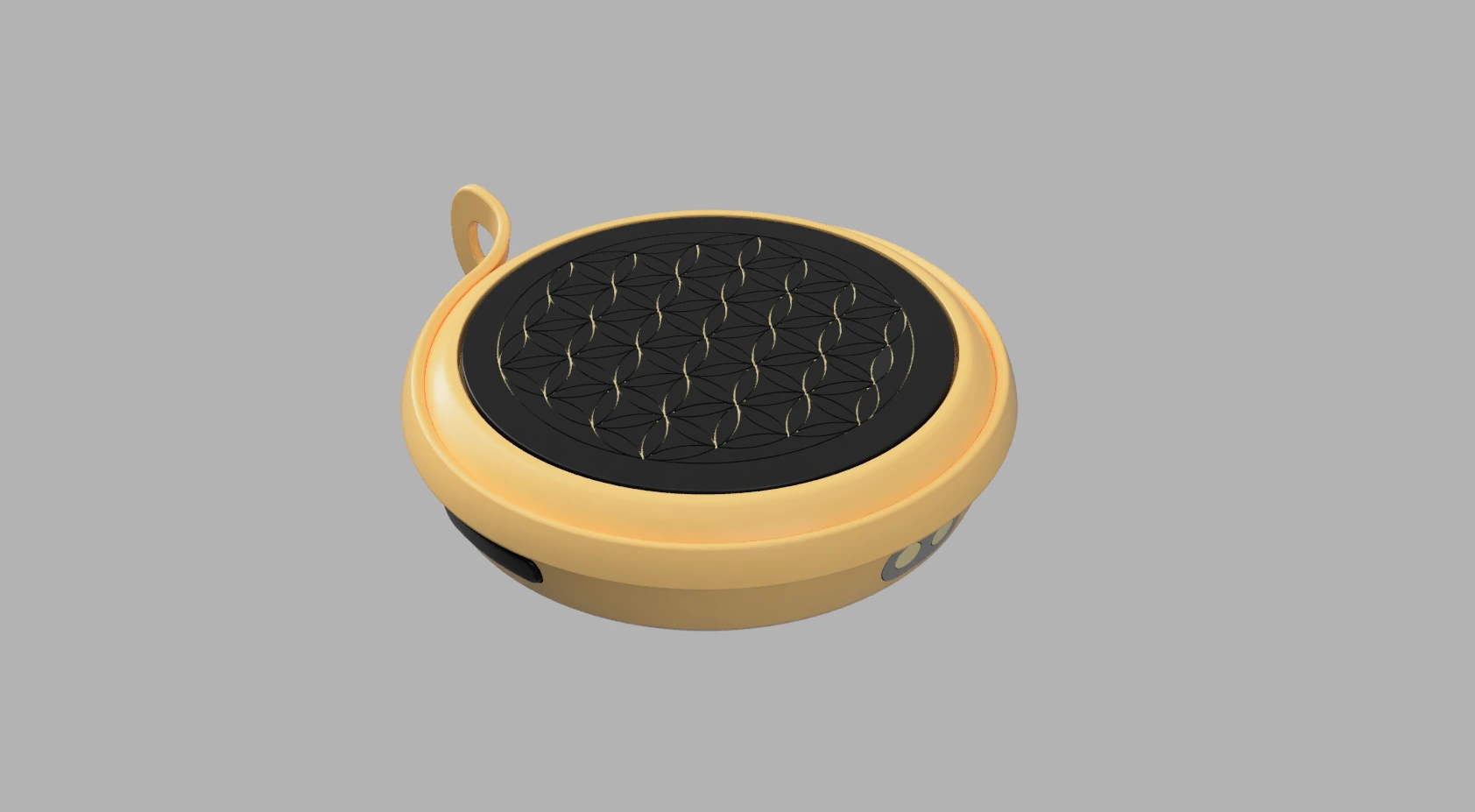
Figure: AI necklace assembled render
6. FAQ
Why was the nRF5340 chosen over a single-core BLE SoC?
The nRF5340 has two independent Cortex-M33 cores. The BLE stack runs on the network core. Audio sampling and all application logic run on the application core. This prevents BLE interrupt handling from disrupting PDM sample timing. On a single-core device, both compete for the same CPU, and BLE jitter corrupts the audio stream.
Why two microphones instead of one?
Noise cancellation. A wearable microphone always captures ambient noise, movement, and clothing contact alongside the voice signal. Two microphones allow the firmware to separate the voice from the background noise. This improves the accuracy of positive self-talk detection on the mobile app.
Why HDI PCB design?
Standard through-hole via PCBs cannot achieve the routing density required at 6mm internal thickness. HDI microvias, blind vias, and buried vias allow full component density on both board sides without the physical constraints of mechanical drill vias.
If you’re building a smart wearable device and facing similar challenges, we’d be happy to help. Feel free to Contact Us for wearable hardware design, embedded firmware, and AI integration services.