
The remarkable property of a dual-rail supply is that compared to the positive DC voltages, whose voltage is positive concerning GND potential, this supply can also provide negative voltage.
DC supplies are more commonly used in everyday electronics than AC supplies. One way to get DC voltage is by converting it from AC voltage or using an energy storage device such as batteries.
With such a voltage, you can power almost every electronic device. But there are exceptions, which are catered by the scope of this blog, “dual rail supplies”.
There are plenty of applications where both positive and negative power supplies are simultaneously required. Examples include audio amplifiers, sensors, Operational Amplifiers, ADCs, DACs, LCDs, and more.
Methods to Generate Dual or Negative Supply
There are many ways to “split” a single supply to behave like a dual supply. Below you’ll read about different approaches and the tradeoffs involved with each approach.
- Inductor-less Charge Pump ICs
- Using a Center Tap Transformer
- Inverting Buck-Boost
- Using a Synchronous Buck
Using Inverting Charge Pump ICS
The topology shown in Figure 1 is known as the inverting charge pump. The working theory of this inverting charge pump revolves around its flying cap C1.
In the first phase, both input switches, S1 and S3, close, and the flying cap gets charged from the input voltage, and the top side is positive, and the bottom side is ground. In the second phase, both the input switches S1 and S3 open, and after some “dead time”, the output switches S2 and S4 close.
This will connect the VOUT to the ground terminal of the capacitor and the circuit ground to the positive side of the capacitor. It is easy to observe that the output side is now inverted, meaning that the ground now behaves as the positive point concerning VOUT, thus creating a negative supply [1].

Practically, MOSFETS are used for switches. However, it is tricky to drive them because of the different voltage potentials at the source. It is easier to use one of the available ICs which utilize this topology to make an inverting supply.
One good example is the ICL7662, as shown in Figure 2. It is a charge pump voltage inverter that will convert a positive input voltage to its corresponding negative voltage by using just an external flying C1 and output capacitor C2.

Pros and Cons
The big problem with these charge pumps is the switching noise which increases with the current draw. Sensitive audio or precision circuits would not like this high noise ratio.
Secondly, this charge pump’s current capabilities could be better than the usual available ICs, only supporting current up to 50mA. However, these charge-pump regulators are smaller, simpler, less expensive, and, best of all, very efficient [1].
Dual Rail Supply Using a Center-Tap Transformer
One way to get positive and negative voltage is by using a centre-tap transformer. A so-called “12-0-12 transformer” is an example of a centre-tapped transformer.
The primary terminals of this centre-tapped transformer are connected to the main supply (220VAC, 50Hz), with the output coming from the secondary terminals. For example, a 24V centre-tapped transformer will have 24VAC across the outer two taps and 12VAC from each outer tap to the centre tap.
Because these two 12VAC supplies are 180 degrees out of phase, it’s simple to make positive and negative 12V DC power supplies out of them.
The benefit of using a centre-tapped transformer is that we can extract both +12V and -12V DC supply from a single transformer [3].

After rectifying this voltage with a full bridge rectifier, we fold all the waves to only one side. Since it is referenced to the centre tap, our GND potential, these voltage values get halved.
That means we got smaller positive waves on the positive side, and on the negative side, we got smaller negative waves.
We can now smooth these waves out with capacitors and a linear voltage regulator to create +12V voltage, also known as a dual-rail supply.
Pros and Cons
The big disadvantage of this design is that AC mains voltage is mandatory, and this whole voltage transformation is less efficient than the charge pump, which we looked at before.
The plus point is that it can supply large output currents, which mainly depends on the transformer size/ current rating. Moreover, since there is no high-frequency switching involved in this circuit, it produces very little or no noticeable noise.
Using An Inverting Buck-Boost Converter
The buck-boost converter is a DC-to-DC converter with an output voltage magnitude greater than or less than the input voltage magnitude.
Here we will look at the Buck-Boost converter, which can operate as a DC-DC Step-Down converter or a DC-DC Step-Up converter depending upon the duty cycle [4].

This converter is an inverting buck-boost converter, i.e., the polarity of the output voltage is reversed compared to the input supply. Thus, it is a negative-output buck-boost converter.
One can also use this for making a dual-rail power supply. If you probe the voltage between the positive of the load and source Vs, you will get +Vs; if you probe across the positive and negative of the load, you will get -Vo.
Many buck-boost ICs available; one example could be LTC3863 from Analog Devices. It can generate inverting voltage using the abovementioned inverting buck-boost topology [5].

Pros and Cons
This topology is a beast if you are looking for high current output. However, it requires several extra components with the IC. But it is worth the cost and design effort since it comes with very low output noise and high efficiency.
Moreover, it’s less complex and allows you to step up or down the output voltage depending on the duty cycle. The only drawback with this topology is the number of components and, thus, additional design effort.
Using a Synchronous Buck converter
The synchronous buck converter is an ordinary buck converter with improved power performance. An ordinary buck converter uses a simple Schottky diode for the conduction period when the switch is open.
However, that diode is replaced by a MOSFET in the synchronous buck. An external inductor, capacitor, and feedback network are required to make a full buck converter, as shown in Figure 6.
The synchronous buck converter is a type of ordinary buck converter with improved power performance. In an ordinary buck converter, a simple Schottky diode is used for the conduction period when the switch is open.
However, in the synchronous buck, that diode is replaced by a MOSFET. An external inductor, capacitor, and feedback network are required to make a complete buck converter as shown in Figure 6.
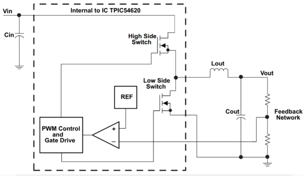
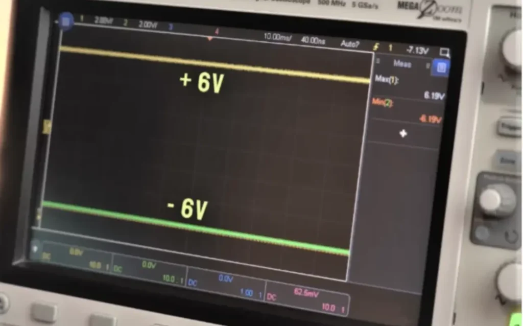
Some nodes need to be modified to make it an inverting synchronous buck converter. The output will now connect to the ground point, and the source of the low-side MOSFET behaves as the output, thus becoming an inverting synchronous converter, as shown in Figure 7 [6].
An example of such a synchronous buck converter is TPS54620. This converter can be modified as an inverting synchronous buck converter [7].

Pros and Cons
This typology is highly efficient compared to the inverting buck-boost topology thanks to the MOSFET’s low power loss.
The integrated MOSFETs allow for high-efficiency power supply designs, which can be positive or negative. The only downside is the complexity of driving two MOSFETS.
Plenty of ICs available, which allows you to not worry about it while designing the supply. These ICs take over the feedback process and provide a stable output voltage.
References
| [1] | R. Keim, “Boosting and Inverting without Inductors: Charge-Pump Power Supplies,” [Online]. [Accessed 2018 ]. |
| [2] | M. Integrated. [Online]. Available: PDF |
| [3] | R. Kansagara, “ +12V and -12V Dual Power Supply Circuit,” [Online]. [Accessed 2017]. |
| [4] | Electrical4U, “Buck-Boost Converter: What is it? (Formula and Circuit Diagram),” [Online]. [Accessed 2021]. |
| [5] | A. devices, “LTC3863,” [Online]. Available. PDF |
| [6] | S. Gupta, “Creating an Inverting Power Supply Using a Synchronous,” June 2018. [Online]. Available: PDF |
| [7] | T. Instruments, “Texas Instruments,” [Online]. Available: PDF |
Facing challenges with Dual Rail supply design or electronic product development in general? Feel free to Contact Us for hardware design, embedded systems, and firmware development services.