Table of Content
ToggleWhat is ESD?
ESD Stands for Electrostatic Discharge. Electrostatic discharge occurs when electricity flows through a conductive body when touched by another charged body.
This usually happens when two charged bodies are in physical contact. In the case of electronics, this phenomenon occurs when the circuit is shorted out at some place, or a capacitor dielectric has broken down.
What harm does an ESD Surge do?
An ESD surge introduces a high current pulse IESD of a few nanoseconds into the circuit board via connections. If not handled properly, this surge can damage the ICs placed on the PCB board.
The voltage VESD that appears across the board components depends on the current surge and its path impedance. Since the current is the independent variable here, we try to vary impedance to mitigate the effects of VESD.
How to mitigate the effects of an ESD Surge?
The simplest way to avoid damage to parts due to an ESD event is to provide it with the easiest path to the ground, i.e. a low-impedance alternate path. The impedance can’t be zero because this can result in shorting of IC being protected.
This is where Transient Voltage Suppressor (TVS) diodes are used. TVS provides the necessary low-impedance path to the ground. The TVS diodes can be used in multiple variations, and several solution configurations are available in the market. A few common connection schemes for TVS are shown in the figure below [1]:
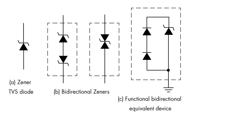
As evident from the figure, the TVS diodes can be used in two configurations, i.e. unidirectional and bidirectional. The unidirectional variant is used when it’s certain that the spike would be prominent on one side, for instance, the current start-up spike.
Furthermore, the polarity of logic is also considered, i.e. if the input data swings to both voltage polarities. However, the ESD spikes and surges tend to be unpredictable in terms of polarity, as do the logic polarity of data pins.
Therefore, bidirectional variants are usually used for ESD protection. For further discussion, the functional device in part (c) will be referred to.
Typically an ESD diode array is connected between the ESD source, i.e. the IO connectors, and the IC to be protected. This is done to give the current an alternate and easy path to ground. This is illustrated in the figure below [2]:
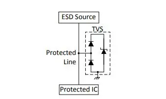
As the voltage across TVS increases, the diode enters the breakdown region. It allows the current to go to the ground. After the appropriate selection of TVS, the next step is to lower the path impedance between the ESD source and TVS ground.
Typical Parasitics in the Path of ESD Source, IC and TVS
The paths joining the ESD source, The IC and the TVS introduce parasitic inductances. These parasitic inductances are illustrated in the figure below:
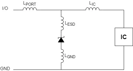
As shown in the diagram above, the paths between the data port, diode and IC have been labelled as separate inductances, and their description is given here:
- LPORT is the inductance between the data port and the rest of the IC and diode assembly
- LIC is the inductance connecting the IC to the diode and the data port
- LESD is the branch inductance for the diode
- LGND is the inductance of the second end of the diode providing a return path to ground
How should these parasitics be handled for ESD Protection?
The following point help in handling the parasitics mentioned above for optimum ESD solution:
- The ratio between LPORT and LIC should be decreased to direct the current to the TVS instead of IC. Conversely, LIC can also be increased to achieve the objective. We can place the IC as far from the TVS as possible (centre of the board). This will increase LIC as compared to LPORT. Furthermore, we should place TVS as close to the Connector as possible, which will reduce LPORT.
- We can also introduce a series resistor between the ESD source and the IC in order to reduce the current flow into the IC. However, care must be taken while using the buffer resistor in case of high-speed lines so that signal attenuation can be avoided.
- To ease the flowing current into the TVS and to the ground, it is necessary to reduce the LESD and LGND. One way of doing this would be to shorten these respective traces.
Reducing EMI Generated from the ESD Surge
Another issue with strong current surges is that they generate strong Electromagnetic Interference (EMI) that can affect the neighbouring signal paths. This is especially relevant for the signals passing from the area between the ESD source and TVS. Such coupling can be seen here [2]:
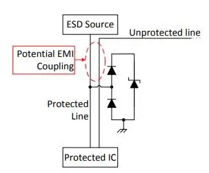
To avoid EMI from interfering with the other signals, we should treat this specific region as a no-go area for other unprotected signals. This is also true for via-connected signals on the adjacent layers that pass through this region.
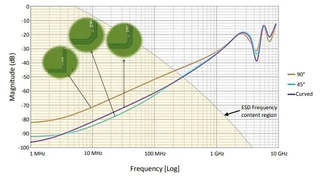
Another important thing to consider in ESD-protected PCB design is the corners between the ESD source and TVS. Corners emit EMI radiations and tend to increase cross-talk on the region. If the corners are necessary, try creating ones with the highest radii (450 being the highest).
The following diagram illustrates the amount of cross-talk between signals caused by 90o, 45o and rounded corners [2]:
To conclude, we have looked at what ESD surges and spikes are and ways to reduce parasitics so that we can effectively use protection solutions like TVS diode arrays. Lastly, we learned about shaping traces to reduce EMI interference and cross-talk between signal paths.
If you are dealing with ESD-related problems in your product or any other safety-related problem, or if you need Consultancy on any Hardware design topic, feel free to Contact Us for our Consultancy. You can check out our other Technical Blogs on various topics or visit our new website Oxeltech.de to learn about our services and products.


