Electromagnetic Interference (EMI) is unwanted electromagnetic energy that disturbs the proper functioning of an electronic device. All electronic devices generate some amount of electromagnetic radiation since the electricity flowing through the circuits is not fully contained.
Table of Content
ToggleHow does Electromagnetic Interference (EMI) occur?
When current flows through a closed path it creates a magnetic field that projects outward and perpendicular to the flow of current. When there are nearby electronic elements or signal paths within this field, Electromagnetic Interference (EMI) occurs.
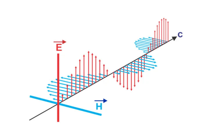
Electromagnetic Waves
Difference Between EMC and EMI
EMC is achieving an acceptable harmony or balance between electromagnetic elements so that the amount of interference is minimal.
On the other hand, EMI is actually unwanted interference from an electromagnetic source. In a nutshell, EMI is the problem and the EMC is the desired functionality of a device to cope us against EMI.
The Sources of Electromagnetic Interference (EMI) on PCB
The sources of EMI can be classified into the following categories:
1. Components
- High-Power Electronic components such as processors, FPGAs, amplifiers, transmitters, antennas, switching regulators, etc. contribute significantly to EMI on the PCB.
- Components with high speed signals can also cause EMI problems such as cross-talk in various sections of a PCB. A high speed signal doesn’t mean higher clock frequency or data rate. It simply means a very fast transitioning between the voltage levels of a signal; or in other words very little rise/fall time. A high speed signal ideally has infinite frequency components and hence it can generate EMI at a vast range of frequencies. A very good example of such a signal is a square wave since it has zero rise/fall times, theoretically. On the other hand, a higher clock frequency just means that the aforementioned EMI disturbances will occur more frequently.
Some of the other forms in which EMI can affect high speed design are radiated and conducted emissions and glitches in the power rails.
2. Signals and Traces
EMI can also be created along signal traces or at pins and connector points. Some of the cases in which EMI problem can arise from signals and traces in a PCB are as follows:
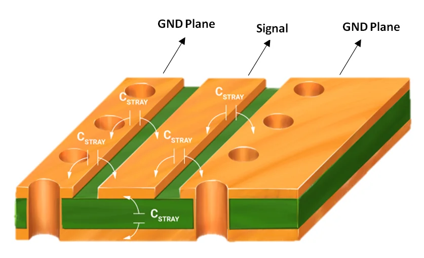
Stray Capacitance in PCB
- Long tracks tend to behave as antennae and they generate radiated emissions when their lengths become a multiple of λ/2 where λ is the wavelength corresponding to the frequency of the signal.
- Unmatched or unbalanced tracks in case of buses and differential signals result in timing mismatch, or clock skew, making the signals reach their destination with different propagation delay. This can cause wrong state of data to be latched and generate faulty results. It becomes especially critical in synchronous protocols such as SPI, USB, CAN, ISA, ATA, and PCI.
- When current enters a circuit, it needs a return path back to its source in order to complete the current loop. If a proper return path is not available to the current, it can use any available path, causing a large current loop area and in turn making it more prone to EMI noise. If somehow this loop area can be reduced, magnetic flux through it will also reduce and there will be a decrease in EMI.
- Unwanted coupling due to stray capacitance between signal paths and ground planes can also cause EMI.
3. External Sources
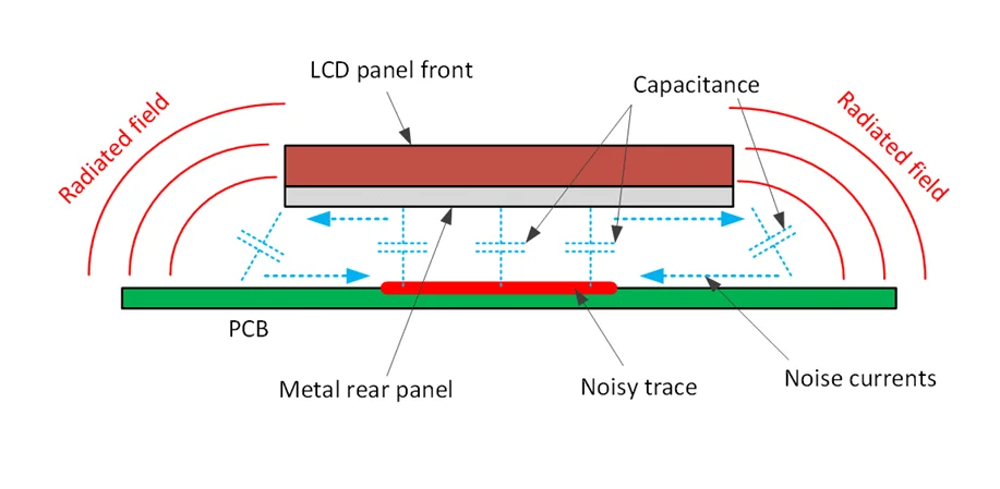
External EMI Sources
- If the PCB is too close to a radiating source which may be another board or element, it can result in EMI on the PCB.
- Harmonics may also be generated by vibrations or movement on the PCB’s environment from other equipment or devices.
- Long off board cables tend to act as monopole or dipole antennae and can result in serious radiate emission problems.
PCB Design Guidelines for Reduced EMI
1. Components Selection:
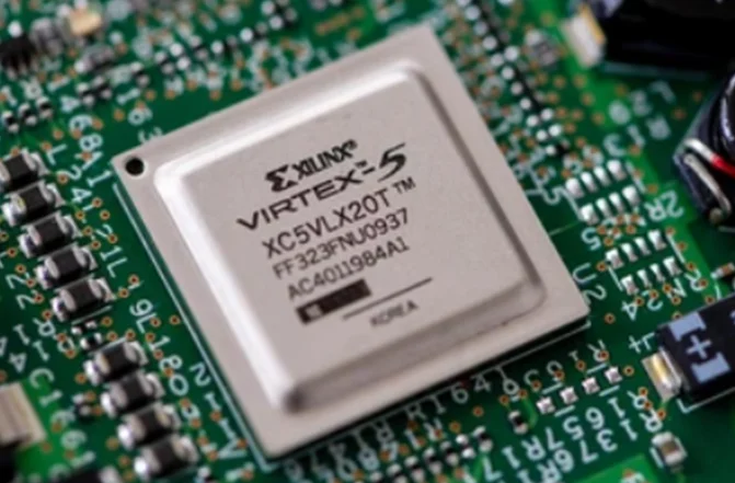
EM Compliant Components (Source: Xilinx)
- Electronic components on a PCB should be categorized according to their ‘Signal Speed’ and ‘Drive Current’, as per the following formula:
- Signal Speed = (fundamental frequency x drive current)/(rise/fall time)
- It’s advisable to compile a spread sheet for each component arranged according to the signal speeds.
- Select low power consumption parts: as often high-power consumption parts are the greatest generator of the EMI.
- Employ heat dissipation techniques: use efficient heat sinks and vias for components that generate heat.
- In order to manufacture cheap off the shelf electronic components, many ICs are available today in plastic casing. However, plastic casing doesn’t do well in shielding against EMI. It is recommended to use components in metal body if the project budget can afford it.
2. Component Placement:
- The highest speed components should be placed on the PCB well away from off board connectors.
- The highest frequency components should be placed in the center of the PCB.
- Isolate different types of components: place components with the same type of signals together such as digital devices should be near other digital parts and isolated from analog devices. This is done in order to prevent current from one section to flow through the other and cause problems.
- Different Sections on a PCB
- Decoupling capacitors of 0.1 uF must be added to all the ICs, between the power and ground pins. These capacitors bypass the high frequency noise. The placement and position of the capacitors help to reduce the current loop area, thereby reducing radiated emissions.
- Position of Decoupling Capacitor (Large Current Loop Area)
- Position of Decoupling Capacitor (Small Current Loop Area)
- Position of Decoupling Capacitor (Small Current Loop Area)
- The oscillator or clock should be placed very close to the microprocessor/micro-controller in order to keep the clock tracks short and minimize emissions.
- If the design includes an EMI filter, it must be placed directly at the point where the DC power enters the circuit.
- All the connectors should be placed along only one edge of the PCB. Any PCB with connectors on two different edges has a high tendency to start behaving as antenna and hence result in radiated emissions.
- Common Mode Radiation with Connectors on Opposite Edges of PCB (Source: ProtoExpress)
3. Ground planes
The ground plane is in many ways your first line of defense against the kind of noise produced by the EMI. Following are some best practices for reducing EMI with ground plane:
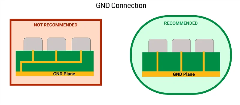
Ground Plane (Source: ProtoExpress)
- Use a multi-layer board: add a layer for the solid ground plane underneath power and signal traces so that the return current will always choose the least impedance path and will form the smallest loop to minimize loop inductance.
- Use split ground planes: The split ground separates analog and digital grounds to avoid noise coupling. When using split ground make sure that the signals from digital circuitry are located entirely over the digital ground and the signals from analog circuitry are located over the analog ground.
- Only connect split ground planes at a single point: The more common ground connections you have, the more loops you create, and the more EMI your design will radiate.
4. Trace Layout
- Avoid using auto-routing as it seriously impacts important signals such as address/data buses, differential signals or other time critical signals.
- Mismatch in the lengths of traces should be avoided for time critical signals, otherwise data and clock will not reach the destination at the same time and wrong state of data may be latched. This is called ‘clock skew’.
- Clock Skew (Source: Cadence)
- Clock signals have the highest spectral content in the system and therefore ground tracks should be manually placed on both sides of the clocks traces to prevent them from inadvertently returning through any unintended path and create radiated emissions.
- Guard Traces on both sides of a Clock Signal (Source: ProtoExpress)
- Keep return paths short: All high-speed signals on a PCB should be referenced to a solid plane. A current flowing in any trace on a PCB must complete the entire circuit loop and come back to the source through the shortest path using the reference plane. If the signal reference is not accounted for correctly, it may lead to potential EMI issues in the PCB.
- Route signals while maintaining references with well-defined return paths along each route.
- For multi-layer boards, different types of signals, such as analog, clock, digital or power, should be allocated on different layers and adjacent layers’ signals are to be routed perpendicular to each other.
- At least a separation of 3 times the width of a trace, or 3W, should be maintained between parallel traces to minimize inductive coupling. A separation of 3W will reduce the cross-talk flux by approximately 70%.
- Trace Separation > 3 * Trace Width (Source: ProtoExpress)
- Avoid buried traces in the ground plane. If you have to use them, put them in the +V plane.
- Do not route the trace near the edge of the reference plane and at least a clearance of 1W must be maintained. If the trace is routed near to the edge of the reference plane, the E-field lines are no longer contained and can leak outside the intended PCB plane can cause the unintended coupling to a trace on an adjacent board within a system.
- Pay utmost attention to how the holes and cutouts in the planes are done. They break up the plane and, therefore, cause increases in loop areas.
- Keep your signals separate: Keep high-speed traces (e.g. clock signals) separate from low-speed signals and analog signals separate from digital signals.
- Keep high-speed traces short: It is especially important to keep the signal input to the receiver path as short as possible, as this line can inject the most “noise” into a system.
- Route differential traces as close as possible: For differential signal paths, it is essential that trace pairs mirror each other. This includes trace lengths, copper weights, and a constant separation. If necessary, meandering should be used to maintain length and separation.
- Avoid sharp angles: Capacitance increases in the 45° corner region changing the characteristic impedance and leading to reflections. This can be mitigated by rounding right angles.
- Avoid Sharp Turns on Traces (Source: ProtoExpress)
- Do not run traces over gaps: If there are gaps in a ground plane, such as near cut-outs, do not run traces over these gaps as the gaps will act as antennas.
- If running the trace over the split reference plane gap is unavoidable then add a stitching capacitor across the split near the trace to provide the high-frequency return path without much deviation across the split.
- Do not place conducting layers next to each other: Never place two conducting layers next to each other in PCB stack-up. It is best to separate these by a ground plane.
- Net changing reference: Usually, high-speed signal traces change multiple layers through vias on the PCB that ultimately changes the trace reference. If the reference change is unavoidable, the two reference planes must be connected through stitching capacitors and/or vias to avoid unintended EMI issues.
- Avoid using vias in differential traces: If you must, use an oval anti-pad shared by the two vias to reduce parasitic capacitance.
- Be cautious with split ground planes: It is best to use separate grounds for different signal types. But make sure that a single point is used to combine the grounds.
5. EMI Shielding
Some specific components on the PCB will inevitably produce EMI, and that can be shielded with a Faraday cage to reduce their effect on other components.
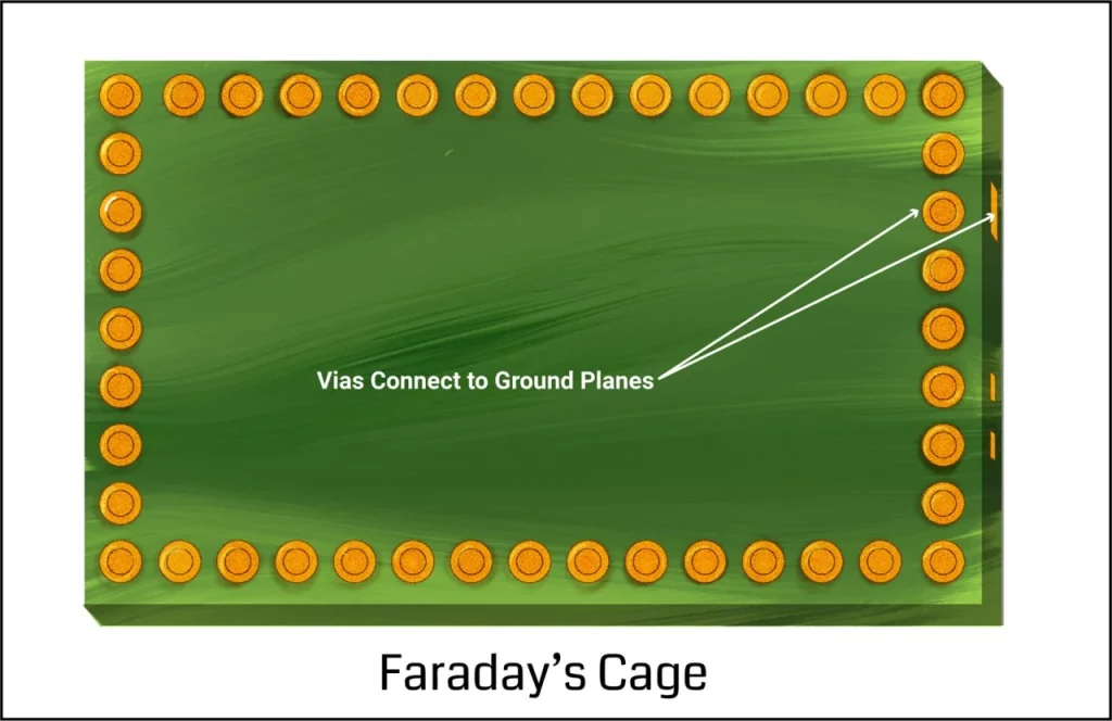
Faraday Cage for EMI Shielding
To reduce EMI from external sources, an enclosure made of conductive materials with sufficient thickness can be used to block RF waves from external sources.
EMI Simulation Tools for PCB
With the aid of simulation, electromagnetic analysis in the design flow of electronic circuits is essential to avoiding expensive reworks. Furthermore, as operating frequencies increase, you cannot make an accurate prediction of PCB performance based solely on circuit performance. Achieving precise designs requires the consideration of physical properties, multiple technologies, interactions, and packaging that only EM modeling and simulation can provide.
Following are the EMI simulation Tools that can help in the identification of EMI in the design:
1. Ansys SIwave:
It is a specialized tool that is used for EMI Analysis, Power Integrity and Signal Integrity of the PCBs.
2. ZUKEN CR-8000:
A PCB simulation and analysis tool for EMI, Power Integrity and Signal Integrity.
3. HyperLynx Design Rule Check (DRC):
This tool helps to determine if the physical layout of a PCB meets the minimum physical spacing and electrical requirements to reduce the likelihood of manufacturing or Signal Integrity (SI) or Power Integrity(PI) or EMI/EMC issues.
4. EMIStream:
It is an EMI suppression tool that can decrease undesirable EMI generated from PCB at an early design stage. The extension of EMIStream is also available in Altium Designer to simulate PCB layout.
References
- Ansys, PCB Design Rules for Electromagnetic Compatibility
- Altium, PCB Design Techniques to Reduce EMI
- Cadence, Techniques to Reduce EMI In Your PCB Designs
- Cadence, The Best PCB Design Guidelines for Reduced EMI
- ProtoExpress
Facing challenges with PCB design for reduced electromagnetic interference (EMI) or electronic product development in general? Feel free to Contact Us for hardware architecture design, embedded systems solutions, and firmware support.

