
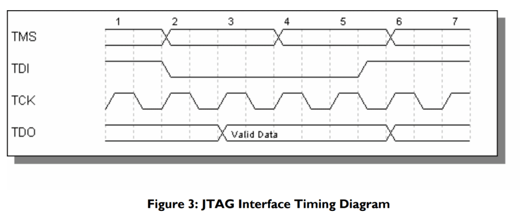
Why Do We Need JTAG?
With recent advancements in technology and shrinking device sizes, it becomes more difficult to be able to test the design and the underlying circuitry. There’s often no space available to attach probes or have test ports if you have to examine the performance and functionality of the device. That’s where JTAG comes into picture. JTAG is a debugging and programming tool. It lets you test your electronic circuit with a minimum access.
But often times, designers face problems with JTAG like connectivity issues. In this article, we’ll explore some of the most common connectivity problems that are faced while connecting to target devices such as microcontroller, processor or FPGA, possible solutions and the factors to consider when choosing the right device.
Common JTAG Connectivity Issues
JTAG is a critical tool used in programming and debugging digital circuits, and ensuring proper connectivity between JTAG and target device is essential for efficient operation. However, there are times when you are not able to get a connection established between JTAG and the target device at all. Or the connection gets lost or the target device stops responding during operation.
Some of the commonly occurring scenarios are as follows:
Incorrect JTAG Configuration
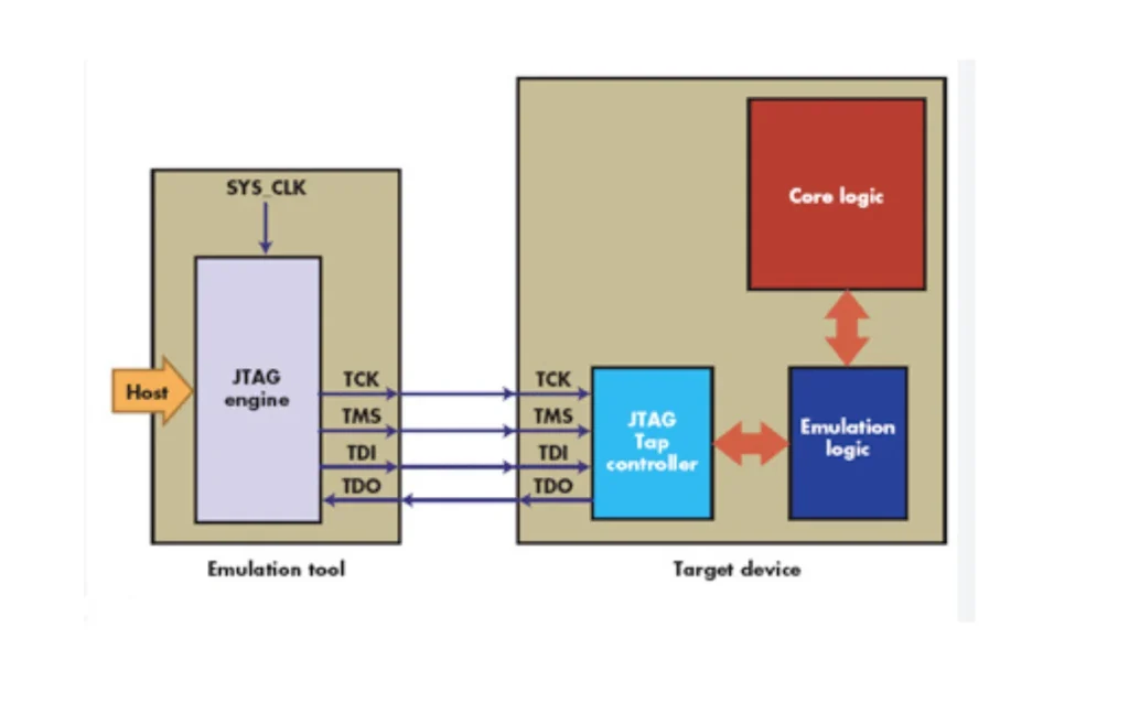
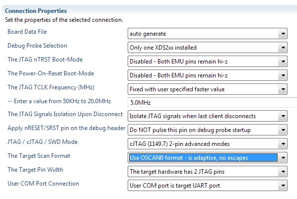
The first and foremost thing to be certain about is to see if the JTAG has been properly configured. In other words, you have to be certain that your debugging environment, such as Code Compose Studio or Visual Studio etc, supports the target device as well as JTAG probe. Furthermore, you have to select the correct model of the JTAG probe family that you are using. For instance, for Spectrum Digital family, you have to select XDS100 or XDS200 or whatever is the type of your probe.
Solution:
- You can check the Target Configuration File to see if your JTAG connection and target device have been properly configured. Do read the device datasheet carefully for these details.
- You can also use Test Connection option to confirm if the configuration has been properly setup and the device is performing correctly.
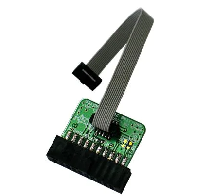
Faulty JTAG Pin Connections
One of the very common reasons of JTAG connectivity failure is a faulty pin connection. This can result in a lot of different types of issues, including no connectivity at all, ‘Cannot Identify Target’, signal interference and erratic data transfer etc.
There can be many reasons for this type of error such as:
- There can be many reasons for this type of error such as:
- Improper or loose connections of the JTAG connector.
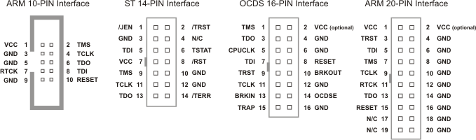
- Incorrect pin connections between the target device and JTAG header.
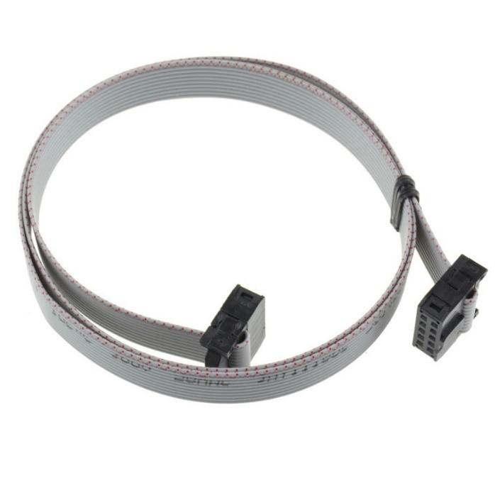
- Broken JTAG cable.
- USB connector of JTAG could be faulty or it may be a charger only connector with no data pin connections.
- USB port of the PC may be faulty.
Solution:
- The obvious solution is to carefully check the cable to see if it’s faulty, broken or has loose ends.
- Check if the JTAG connector is properly attached to the PCB.
- Pin connections should also be verified by checking it against your schematics to confirm that the pins are attached to the appropriate ports on the target board.
- The best approach is to incorporate such check points in the design procedure and once again in the PCB layout stage.
- You can also plug the USB end of cable to a different port of your PC.
Voltage Mismatch and Power Supply Issue
One of the basic JTAG related issues is voltage mismatch and power supply problems. Straightforward as it may appear, but such type of issues can result in ‘Target not responding’ error, erroneous behavior, device failure and even permanent damage to target device. Some possible scenarios as are as follows.
- The operating voltage level of the target device may not be compatible with the JTAG. For example, the JTAG may be operating on 5V or 3.3V whereas your target device may be operating on 3.3V, 1.8V or 1.5V.
- The power supply being used may be faulty and can cause fluctuations, over voltage, under voltage, noise or even total power loss. This kind of problems can lead to data loss, delays in programming and even permanent deformation to the device.
- The device may not power up at all if it is not receiving any voltage at all.
Solution:
- a. See the datasheet of the device and make sure that the JTAG is compatible with the operating voltage of device.
- b. One way is to deal with voltage mismatch is to utilize a voltage translator or level shifter.
- c. A JTAG debugger that supports a wide range of voltage levels and can be used with different CPUs and FPGAs is another option.
- d. Make sure that your power supply is giving a stable output. It’s better to use a power supply that has recently passed QC tests.
- e. Power supply issues can also be tackled by the use of regulators, filters, and surge protectors. A thorough analysis of the system may also be performed to identify potential power supply issues.
Reset Signal
Reset signal is one of the most important signals in any embedded device and any discrepancy with reset can cause in a variety of different unwanted outcomes some of which are as follows.
- • It is possible that the target device may not be receiving the correct reset signal or receiving it at an inappropriate point in time.
- • Sometimes, the device is not able to come out of the reset state while at other times, the device may not respond to the reset signal. This can result in ‘Target not responding’ error.
- • In case of flash based target devices, a pre-loaded piece of code in the flash or a faulty application can result in sending reset signal continuously and hence sabotages the overall intended operation. This sort of scenario can cause errors like ‘Device not recognizable’ or ‘Invalid Device ID’.
Solution:
- a. Check the reset signal for continuity and see if it actually reaches the target device.
- b. You should also monitor the timing of the reset signal and its shape as it could have deformed or deteriorated by EMI or some other noise source.
- c. For flash based target devices, changing the boot mode of device or a complete erase of flash can work.
Clock Speed Mismatch and Clock Stability
Another type of JTAG related connectivity problems is when there is a mismatch between clock speed of JTAG and that of the target device. This can lead to timing problems and possible data corruption. The root cause of this issue can be several factors such as differences in clock frequency, phase, or skew. Following are a few of the possible fault scenarios.
- The JTAG clock speed must be compatible with that of the target device. A possible way to make this mistake is to configure the JTAG clock speed to be too high for the target device.
- Another scenario is that the JTAG is configured for fixed or adaptive clock but the same is not supported by the target device.
- It is also a possibility that the clock signal was not routed on the board at all and hence it cannot reach the device.
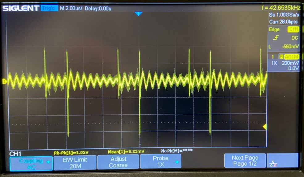
- Clock stability is another important factor which means that clock signal is not clean but jittery or skewed. In this case, the target device is not able to get correct timing information from clock signal.
These issues can result in ‘Dead JTAG Clock’ error.
Solution:
- Please consult the datasheet of the device to confirm compatible clock speed for the said device and also check if the device supports fixed or adaptive clocking.
- Double check the clock signal on the board to ensure proper connection.
- Keep the length of clock track short and try to keep it away from the noisy signals.
- Using a clock buffer can reduce signal deterioration and delay brought on by lengthy tracks on the board.
- It’s critical to guarantee that the clock signals have clean signal integrity because erroneous signal integrity can result in a mismatch in the clock speeds.
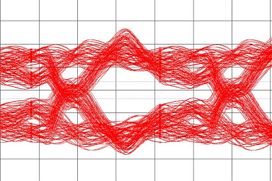
Poor Signal Integrity Issue
When dealing with JTAG connectivity to a target device, poor signal integrity can be a significant issue. This occurs when the signals that carry data between the devices become distorted or degraded, leading to communication errors and potential data loss.
- A common cause of poor signal integrity is the length of the JTAG signal traces. Longer traces can introduce more noise and interference, which can impact the signal quality.
- Similarly, the length of JTAG cable also affects the signal integrity and correct operation. If the length of the JTAG cable exceed by 50 cm, it is more susceptible to interference and noise.
- Another possible issue is electromagnetic interference from nearby devices, which can cause signal distortion.
- The mismatch between transmission line impedance and load impedance can cause a signal to partially reflect back towards the transmitter. This reflected signal can cause interference and degrade the signal integrity, which can result in incorrect data transmission.
Solution:
- The length of JTAG signal traces on the board needs to be kept smaller in order to keep signal integrity intact.
- To address poor signal integrity, designers can implement techniques such as impedance matching, shielding, and signal buffering. Impedance matching can help ensure that signals are transmitted at the correct voltage level, while shielding can help prevent electromagnetic interference.
- Signal buffering can improve signal quality by amplifying weak signals or reducing strong ones.
- If the length of the JTAG cable goes beyond 50 cm, decoupling capacitors may be used with each JTAG signal to keep it as clean as possible.
- Signal reflections can be controlled by using terminations or impedance matching.
EMI Related Issues
Connectivity issues can also arise due to electromagnetic interference (EMI). This can cause signal distortion and loss, resulting in failed connections and communication errors
- To reduce EMI, one solution is to ensure that all electronic devices are properly shielded and grounded.
- Additionally, using properly shielded and twisted cables can help reduce signal noise.
- Another option is to use signal boosters or repeaters to strengthen the signal and compensate for any loss.
- It is also very critical to make sure that the JTAG interface is not linked to any other devices or interfaces that could interfere with its operation. To avoid interference, other interfaces or devices may need to be disabled in some cases.
- Finally, identifying the source of the interference and taking appropriate measures to eliminate or minimize its effects is critical to resolving interference issues with JTAG connectivity. Proper grounding, shielding, cable management, and careful placement of devices can all contribute to a stable and reliable JTAG connection.
PCB Layout Design Issue
Connectivity issues between JTAG and target device on a printed circuit board (PCB) can arise due to PCB layout design issues. Problems such as signal reflections, cross talk, EMI, noisy ground planes or tracks and longer track lengths can all result in sabotaging JTAG connectivity and performance.

Solution:
- To solve these problems, proper PCB design practices must be followed, including placing decoupling capacitors near the power pins of the processor and FPGA.
- Use of a ground plane to reduce noise, and ensuring proper routing of JTAG signals is also very important.
- Additionally, reducing the trace length of JTAG signals can also help to minimize signal degradation.
- Ensuring the correct impedance of the traces and adding termination resistors can also improve signal quality.
Conclusion:
JTAG is a valuable tool for programming and debugging embedded systems, but it presents various challenges that can hinder its debugging and programming capabilities, particularly when dealing with custom designed boards. However, by carefully selecting the appropriate device and ensuring proper connections and configurations, developers can effectively mitigate potential issues, ultimately saving valuable development time during the programming and debugging process.
Facing challenges with JTAG connectivity, debugging issues, or embedded hardware development in general? Feel free to Contact Us for firmware development, hardware debugging, and electronics design assistance.