Altium Designer is considered the epitome of EDA tools for hardware design engineers when it comes to professional schematic and PCB design. It is inclusive and encompassing as far as all the steps in the design and management process are concerned.
This series of articles has been divided into three parts based on the design stage, i.e., design process tools, project management tools, and collaboration tools.
In this second article of the series, we’ll cover tools that set Altium apart from other tools for schematic and PCB project design management.
Table of Content
ToggleProject Management Tools
1. Active BOM:
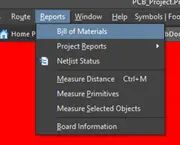
Bill of Materials or BOM can be generated in two ways in Altium. On way is to go to the Reports tab and generate ‘Bill of Materials’. This gives you a specified set of attributes that will be included in the Excel sheet.
The alternate method is through the ActiveBOM utility provided by Altium. ActiveBOM is an interactive way of creating and maintaining BOM during the design and sourcing phase of the project. ActiveBOM can be generated by going to ‘Project’ tab, selecting ‘Add New to project’ and clicking ‘ActiveBOM’.
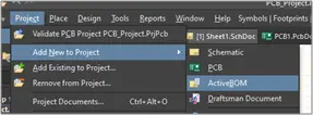
A new file will be added to project documents list with BomDoc extension.
- ActiveBOM provides a flexible real-time view of the BOM during the design phase. If a new component is added, the ActiveBOM will be automatically updated.
- Another cool feature is maintaining the part choices for each device in the schematic. You can have a primary solution and several secondary solution. If you click on any row in the ActiveBOM document, you’ll see a primary solution with supplier information in the bottom tab.

- You can add alternate choices by going to Add Solution button, selecting alternate part number and click OK.
- You can also prioritize the solution list by giving each solution a Star rating. The solution with the higher rating will be displaying as primary solution and others as secondary solutions. In this way, you can change solutions if there is an availability issue with the primary one.

2. Design Rules Wizard:
Generally when we are setting design rules for schematic and PCB design, the design rules apply to every entity placed on the board. This restricts the user from customizing his rules based on the nature of the circuit block i.e. power supply or Analog/Digital circuitry etc.
Altium resolves this issue by providing Design Rules Wizard in which you can set custom design rules for specific Nets or Net Classes on the board. These rules can also be prioritized in comparison with normal rules as per requirements.
Steps for Setting Custom Rules:
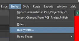
- Rules Wizard can be accessed by going to Design tab and selecting ‘Rules Wizard’.
2. On the next window, we can select constraint type such as ‘Clearance Constraint’.
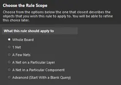
3. After selecting constraint type, scope window opens up in which we can limit the scope of rule to individual Nets, Net Classes or the entire board etc.
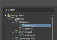
4. After setting the rule, the rule should show up in the ‘Rules’ list. The priority of each rule can also be prioritized in the same window.
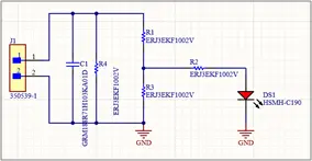
For the sample circuit given below, a custom rule for GND Net has been set which has higher value of clearance constraint.
The priority of the GND rule is set higher than the normal rule. After the application, the PCB copper is poured. The output is given here:
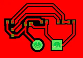
We can see that all the GND Nets and Pads have higher clearance than the rest of the nets.
3. Release Management
After the completion of a PCB design, the final task usually is to send appropriate files to the fabrication/assembly house for fabrication and assembly of PCB. Altium Release Management features provides extensive help in this regard. You can select files for different functions or tasks and this tool neatly organizes the appropriate fabrication output files for the fabrication/assembly house to use.
Steps for Generating Fabrication Outputs
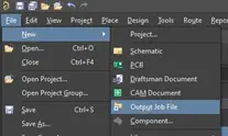
1. To generate files, you have to create an output job file. Go to ‘File’, select ‘New’ and click ‘Output Job File’.
2. Select the output files that you need to be exported and connect them to containers of your choice i.e. either in PDF format or in separate folders. To do this, you have to first click on container type and then click on the files that go with that format.
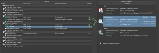
After finishing the connections, click on each container type and click ‘Generate Content’. The generated outputs will be at the path specified in the container box.
3. SmartPDF
Altium offers an interactive version of PDF that can be generated known as Smart PDF. In this version of PDF, devices are clickable and their properties can be checked upon clicking. Furthermore, we can efficiently search a particular part by its name, designator or any other parameter.
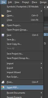
SmartPDF can be generated by going to ‘File’ tab and clicking ‘SmartPDF’:
For any Altium or PCB layout related issue, or any Hardware Design related challenge in general, feel free to Contact Us for our consultancy. You can check out our other Technical Blogs on various topics or visit our new website Oxeltech.de to find all about our services and products.


