Altium Designer is considered the epitome of EDA tools for hardware design engineers when it comes to professional schematic and PCB design. It is inclusive and encompassing as far as all the steps in the design and management process are concerned.
This series of articles has been divided into three parts based on the design stage, i.e., design process tools, project management tools, and collaboration tools.
This article will cover tools that set Altium apart from other tools for the schematic and PCB design process.
Table of Content
ToggleDesign Process Tools Shortcuts:
Quick Zoom
During the design process, you can quickly zoom out and fit your document dimensions by pressing ‘V’ for View and then ‘F’ for Fit. This will automatically adjust your View to document size.
Exact Coordinate Access
During part placement or polygon placement, there is a requirement to have access to exact coordinates for accuracy and aesthetics. This can be done by pressing ‘J’ for Jump and then ‘L’ for jumping to that location. A window will open up for you to enter coordinates.

Now when you press ‘Enter,’ your cursor will be at the entered coordinates.
Visibility
During PCB design, you often have to switch visibility to check your placement routing with reference to other layers. For this, you can use the Shift+S command. Let’s take an example to show how this works. Here is a PCB cutout:
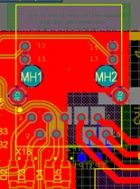
When you press Shift+S once, this View changes to the following View in which the top is highlighted and the layers underneath are in the faded form:
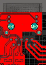
Now, if you press Shift+S again, the visibility shifts to the selected layer (top layer in this case), and the rest are switched off:
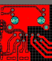
4. Repour Polygons
During PCB design, we must shelve and re-pour polygons and planes from time to time. To re-pour all the polygons/planes, you can press T for Tools, G for Polygon Pours, and then A for re-pour All.
5. Wire
To toggle the Wire tool for connecting devices in Schematic or routing in PCB, the Ctrl+W shortcut can be used. The cursor will change to Cross upon using this shortcut.
6. Highlighting a Net
Keep pressing Shift and hovering over the net in question to highlight a net. The entire net can now be seen clearly because it has been highlighted for focus.
Parameter Manager:
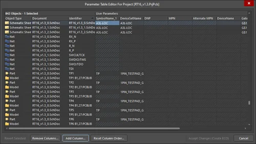
Parameter Manager is a feature using which we can add and modify parameters in the project. Parameter Manager can be accessed in the Schematic window by selecting the Tools tab and clicking Parameter Manager:
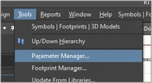
We can edit individual parameters and all the parameters based on their category. Furthermore, new parameters can also be added.
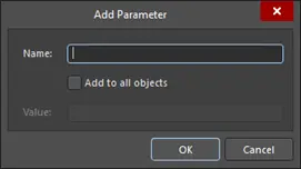
To add a new parameter, you have to click on the ‘Add Column’ button, and the following dialogue box opens up in which you add the name, association, and value for that column:
Pin Mapping Visualization Tool:
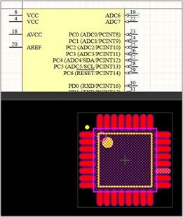
Reviewing the pin mapping for microcontrollers and other ICs with multiple pins takes time to quickly check the mapping of the schematic symbol and the PCB footprint side by side.
Steps for Checking Pin Mapping
- Open the integrated library you created for the project and the part you want to check. The window that opens up shows both symbol and footprint.
- Now, if you click on any pin in the symbol, the corresponding pin in the footprint will be highlighted. In this way, you can verify the pin connections using the datasheet.
PCB Filter:
During the PCB design process, there comes a situation when you have to perform a task on several objects of the same type all at once. In this case, performing the same task separately on each object becomes quite tedious.
Altium’s PCB Filter is a huge help in this scenario. You can add filters on different object types, such as designators or component types, such as vias or nets, etc., and then perform the intended task on them all at once.
Steps for Setting Filter and Performing a Task
- Select ‘PCB Filter’ from the bottom left.

2. You can add specific filter commands in the ‘Filter’ section. For instance, we want to change the size of all designators on the board. We’ll write ‘isdesignator’ expression in the section and check the ‘Select’ check box.
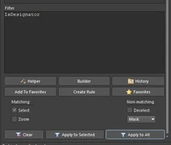
You’ll see that all the designators have been highlighted.
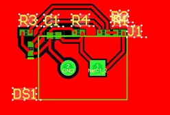
Now you can go to the properties and change the required parameter. Another example for these types of tasks, is changing via size of all GND vias.
Alternate Method of Collective Editing
You can perform the same collective action through another method.
1- Now if you want to change designator size, you can go to the String Type Object for designators and change status from ‘Any’ to ‘Same’.
2- Right-click on the object that needs to be altered and click on ‘Find Similar Objects’.

The following window should open up.
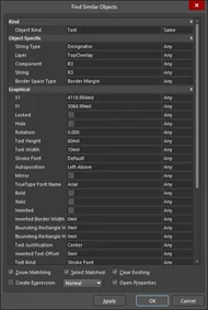
Now when ‘OK’ is pressed, we can see that all the designators are selected and we can go to ‘Properties’ tab and perform changes as we did in PCB Filter method.
For any Altium or PCB layout related issue’s, Firmware Development, or any Hardware Design related challenge in general, feel free to Contact Us for our consultancy. You can check out our other Technical Blogs on various topics or visit our new website Oxeltech.de to find all about our services and products.

