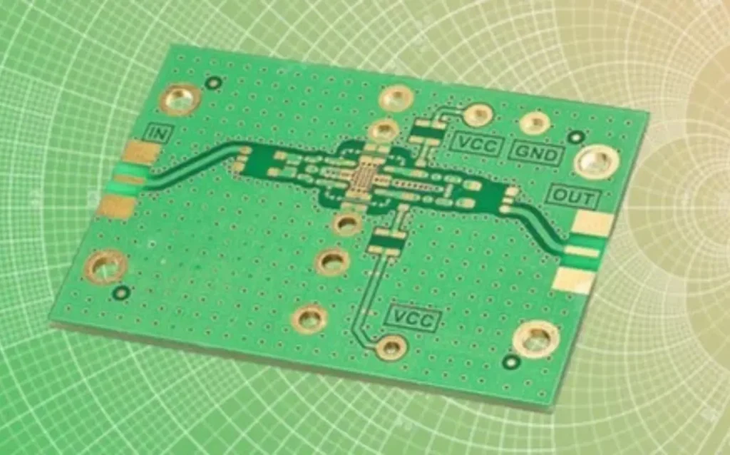
Grounding is the first line of defense against Electromagnetic Interference (EMI). Design for Electromagnetic Compatibility (EMC) involves utilizing techniques like EMC filters, shielding and circuit partitioning to ensure good EMC performance. However, properly planning and implementing grounding in your design, effectively reduces emissions, common mode noise and interference due to capacitive and inductive coupling and thus improves overall performance against EMI.
Table of Content
ToggleWhat is Ground?
By definition, a Ground is a point or an equipotential plane in a circuit that provides a reference potential or 0 V against which all the voltages in the circuit are measured. It can also be defined as a physical connection the earth, meant to protect the circuit against faults.
However, in terms of functionality, there’s another way in which ground is defined and understood by Electrical Engineers. The common return path for all the currents in a circuit is also termed as ground.
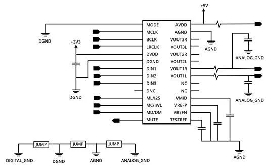
Ground in an Electronic Circuit (Source: LearEMC)
Although some experts consider this a mere confusion and emphasize on calling it the ‘return path’ for better conceptual visualization, the practice has become so common these days that both these terms are used interchangeably.
Grounding for EMC
Where proper grounding vastly improves the EMC performance of a circuit, poor grounding can make the existing performance even worse and cause problems such as common mode noise and signal interference. A recent study has shown that poor grounding has been a leading cause of EMC failure in electronic devices.
The key idea of proper grounding is based on the fact that all the currents in the circuit must return to their source without disturbance and mainly through the path planned for return. Therefore, it comes down to two parameters:
- Ground Impedance
- Current Loop Area
If the impedance of planned ground path is low, the signals can easily return to their source without much disturbance and causing havoc to neighboring signals. Similarly, smaller current loop area minimizes interference and keeping the induced voltage as low as possible.
Grounding for EMC (Source: Cadence)
Therefore, the grounding should be designed so as to keep the return paths well defined and localized.
Grounding in PCB
Grounding in a PCB can be considered as one of the most important system level consideration in complex systems. The grounding strategy and implementation on PCB can be the deciding factor for that design to pass EMC.
Before going any further, it is important to understand how energy flows in a PCB.
*How Does the Energy Flow Through a Circuit in a PCB
In a PCB, electric energy does not flow as electric current through the copper tracks or planes. On the contrary, this energy flows as electric (E) and magnetic (H) through the dielectric of the PCB. The copper tracks or micro strips along with the nearest ground plane steer this electromagnetic energy from one point to the other. Hence, it can be said that the copper tracks and planes essentially behave as a waveguide for electric energy because these tracks guide the energy through the dielectric core of PCB by offering it a path of least impedance.
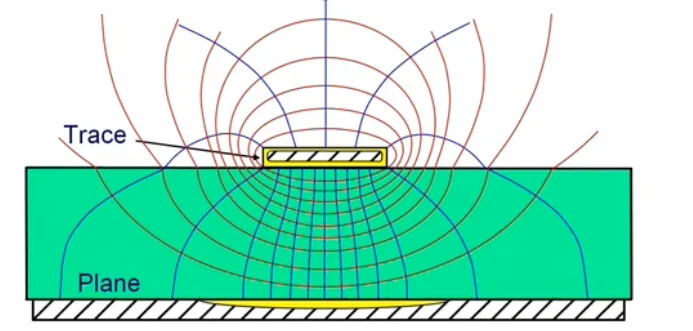
Spreading of Field Lines from Top Layer (Source: Rick Hartley, Altium)
As these fields move through the PCB, it generates a forward current and a return current simultaneously. So, at any point in time, a forward current and a return current both exist. This clearly indicated the importance of return path. Since we use direct connection to ground plane through vias in multi layer boards, we assume that the return current follows a direct straight line path back to its source in the ground plane from through vias. That’s true for DC and lower frequencies but at higher frequencies something else happens.
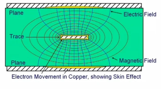
Spreading of Field Lines from Inner Layers (Source: Rick Hartley, Altium)
To have a clear idea, consider the following figure. It shows a 2-layered PCB with ground plane at the bottom layer and a track that routes from the IC at the top right to the bottom right. Although the track goes all around the PCB to get to its destination, the ground connections of both ICs are directly connected to the ground plane at the bottom through vias.
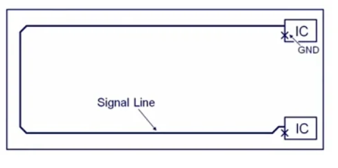
Return Path of Current in 2-Layer PCB (Source: Rick Hartley, Altium)In case of DC or lower frequencies up to few kHz, the return current will directly go to the ground plane through one via and go to its source IC in a straight line, as expected. But at higher frequencies, say from 100 kHz and above, the return current will go directly beneath the track and travels all the way back to its source. Apparently that’s a much longer path, given there are vias available.
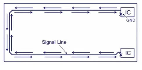
Return Path of Current in 2-Layer PCB (Source: Rick Hartley, Altium)
The reason for this is Ground Impedance.
Ground Impedance
The return current will always choose a path of lowest impedance. It is important to keep in mind that the return current doesn’t always follow the path that we have assumed it will follow. It may follow a completely different path especially at higher frequencies due to the impedance of the ground plane.
The ground impedance is not purely resistive but has inductive as well as capacitive components. Since copper track and ground plane, with dielectric core in between, act as waveguide for electrical energy, the Inductive element of its impedance hinders this flow whereas the capacitive element supports it. Therefore, the ground impedance is give by the following formula:
Zo = √(Lo/Co)
And for higher frequencies, this value changes to:
Z = √(R + jwLo)/(G + jwCo)
From above relation, it is evident that for higher frequencies, the path of lowest impedance will be exactly between the copper track and corresponding ground plane.
Consequently, we can conclude that in order to ensure that the return current chooses the designed path we must have a ground plane very close to the signal layer. This way the electromagnetic fields will stay confined in the space between the track and ground plane. On the contrary, if the ground plane is not close enough, the fields will spread out causing interference with other nearby signals on the same signal layer or with the signal on the adjacent available layer.
Implementation
Keeping in view the above concept, let’s see how we can make use of this information to design better grounding for our PCBs and get better EMC performance.
- Layer Stack UpThe high speed and high frequency designs of today make the job of PCB designer much more challenging, especially when we factor in the EMC performance. A good stack-up gets half the job done for you.Our main goal is to keep the electromagnetic fields on the PCB confined in a local space so as to not disturb other signals. This can simply be done by ensuring that each signal layer has a return path which can be a copper pour or plane, available right next to it.Poorly Designed Layer Stack (Source: Rick Hartley, Altium)The above layer stack of a 4-layer PCB is a poor design because for signals on layer 1 and layer 2, the ground plane is too far away and a lot of interference and common mode noise will be generated.Poor Designs of Layer Stack in 6-Layer PCB (Source: Rick Hartley, Altium)The above figure shows layer stack of 2 different 6-layer PCBs and both of them clearly have the same problem. The one on the left side has ground plane on layer 3 which will make signals on layer 1, 5 and 6 difficult to couple and hence emissions will increase.Good Designs of Layer Stack in 6-Layer PCB (Source: Rick Hartley, Altium)Figure above shows two layer stacks from 2 different PCBs. These are the examples of good layer stack arrangement as each layer has an immediate access to a ground plane.
- Ground PlanningThe golden rule here is to never split your ground plane. Always try to have a solid and clean ground plane. However, there can be instances when one has to split the ground plane. For instance, if you have both analog and digital components on the same PCB and you have an analog ground AGND and a digital ground GND. In such cases, make sure that the circuit components and their tracks from one section of PCB must have an undisturbed section of the corresponding ground plane beneath it.The following case study was presented by Prof. Tzong-Lin Wu from National Taiwan University in which he presented 4 different scenarios in a 2 layer board. The top layer has only copper track while the bottom layer is ground layer.In case 1, the ground plane is a solid copper plane. Case 2 has a split in the ground plane perpendicular to the track on layer 1. Case 3 has many small perforations or windows on ground plane but the section of plane under the layer 1 track is undisturbed. Finally, case 4 has perforation or copper free area under a part of the layer 1 track.Effect of Splitting Ground Plane (Source: Prof. Tzong-Lin Wu, National Taiwan University)During the EMC testing, the following results were observed.Effect of Splitting Ground Plane on EMI (Source: Prof. Tzong-Lin Wu, National Taiwan University)Case 1 has the best EMI signature while case 4 has the worst. Case 3 is almost as good as case 1 because it has undisturbed ground plane beneath the track although the ground plane was not solid. Case 3 has worse performance but it is still better than case 2 where the perpendicular split caused the field lines to go haywire.Effect of Splitting Ground Plane on Current Patterns (Source: Prof. Tzong-Lin Wu, National Taiwan University)The above figure shows the current patterns in each case and they show how the field lines are adversely affected by the split.
- Proper Sectioning of PCBAs discussed in the previous section, it is extremely important that if there are more than one type of circuit components, such as analog or digital components, or even if all of them are digital but they are not referred to by the same ground plane, then we must make different sections of the PCB and ensure that not just the components but also the related signal tracks must stay in their own sections.PCB Partioning (Source: Rick Hartley, Altium)
- Use of GND ViasIn case the signal on a certain layer has to go to another layer, make sure that the next layer is on the other side of ground plane so that the signal track stays in the close vicinity of the same ground plane as shown in the figure below.Use of Ground Vias (Soucre: Rick Hartley, Altium)For the case when it is not possible for the signal track to stay on the layer right next to the ground plane, rather it has to go to a farther layer with a different ground plane, a ground via connecting the two different ground planes must be placed near the point where the track leaves the layer. That ground via acts as a bridge between the two ground planes.Use of Ground Vias (Soucre: Rick Hartley, Altium)Use of Ground Vias (Soucre: Dr. Howard Johnson)For more sensitive or critical tracks, a GND via or more than one GND via must be placed nearby the tracks to contain the fields. If it is not possible to place even one GND via near each track as in high density PCBs, then at least one GND via must be placed in the center of a group of tracks.
Conclusion
The electric energy does not flow through the copper tracks on a PCB rather it flow through the dielectric core of the PCB contained between copper tracks and ground plane. Return path of the currents is very important and has to be managed very carefully. The sole purpose of ground planes in context of EMC is to contain the electromagnetic fields to minimize EMI and common mode noise. If one has a clear idea of how the fields are going to behave, any circuit can be implemented on a PCB without having to worry about EMI.
For any queries or information regarding the topic or other topics related to Embedded Systems, feel free to Contact Us.
References:
- Rick Hartley, Altium
- LearnEMC.com
- Cadence.com
* The concept of flow of electric energy in PCBs is discussed in much more detail by Rick Hartley.

