
Source: Pixabay
Wearable devices combine sensors, wireless communication, batteries, and processing within a very small space.
In many projects, PCB design becomes one of the most challenging parts of the system, mainly because multiple constraints need to be handled simultaneously.
Below are some of the key PCB design challenges in wearable electronics and what needs to be considered during development.
1. Limited Board Area
Wearables require very compact PCB layouts.
Common approaches include using small packages such as WLCSP or QFN, selecting highly integrated ICs, and minimizing connectors.
While these help reduce space, they also introduce trade-offs. Smaller packages increase assembly complexity, and fewer connectors make debugging more difficult.
In practice, component selection has a direct impact on how feasible the PCB layout will be.
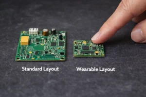
Figure: Standard vs compact PCB layout
2. Battery Dominates the Volume
In most wearable devices, the battery occupies a large portion of the available space.
As a result, the PCB layout is often designed around the battery rather than the other way around.
High current paths need to remain short, and RF sections should be separated from power areas to avoid interference.
A common mistake is treating the battery as a secondary element, whereas in reality, it defines the overall layout strategy from the beginning.
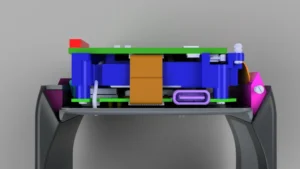
Figure: Battery-dominated PCB in wearable electronics
3. High Routing Density
Limited space leads to tight routing conditions.
To handle this, designers often use HDI stackups, microvias, or via-in-pad techniques, along with careful power plane planning.
These approaches improve routing flexibility but also increase manufacturing complexity.
The key decision is not just how to route the board, but whether the chosen approach aligns with the product’s complexity and constraints.

Figure: High routing density in PCB
4. Antenna Performance Near the Human Body
Wearable antennas operate close to the human body, which can affect signal performance.
Maintaining proper ground clearance around the antenna and separating it from battery and power sections is important.
A common issue is that the device performs well in lab conditions but behaves differently when worn.
For this reason, RF performance should be validated early under real usage conditions.

Figure: Signal attenuation near the human body (Source: hybratech)
5. Thermal Management
Wearables are in direct contact with the skin, so heat must be carefully controlled.
Heat can be managed by spreading it through ground planes and controlling peak current through firmware.
In many cases, thermal behavior is influenced by the entire system rather than a single component.
This makes thermal management a combined hardware and firmware consideration.
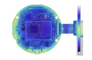
Figure: Thermal Distribution Simulation of a PCB
6. Mechanical Integration
In wearable devices, PCB design is closely tied to mechanical and industrial design.
This often involves rigid-flex PCBs, curved layouts, or custom board shapes.
Because of this, PCB and enclosure design need to evolve together. Changes in one will often impact the other.
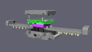
Figure: PCB and Enclosure Mechanical Integration
Conclusion
PCB design in wearable electronics involves balancing multiple constraints, including size, power, RF performance, thermal behavior, and mechanical requirements.
In most cases, the real challenge is not a single limitation, but how these factors interact and influence each other throughout the design process.
Facing challenges in wearable electronics or PCB design for compact devices? Feel free to Contact Us for electronic hardware design, embedded designs, and firmware development services.